1Learning Outcomes
Define the components of a Finite State Machine (FSM).
Describe how circuits can be represented as FSMs.
Describe how FSMs transition between states.
Express an example sequence detector circuit as a waveform diagram, FSM, truth table, and circuit.
🎥 Lecture Video
Finite State Machines (FSMs)[1] are a useful abstraction for many types of computing tasks. These show up in many areas of computer science and are often used in hardware design. As an example, for a hardware controlled cache in a processor design, a FSM would be used to control the set of actions associated with servicing loads and stores from the processor. It would go through a series of “states” as it responds to requests from the processor, as times needing to access main memory and put new data into the cache. We can imagine describing the cache behavior as an algorithm or program, and this algorithm would be implemented in hardware with a FSM!
2Finite State Machines
A FSM has a set of inputs, a set of outputs, and a finite collection of states. At any point in time, the machine is in one of the states. Each state can have one or more arcs that takes the machine from the current state to a new state when certain input values appear. Output values are associated with arcs, meaning that when a machine leaves a state, it can change its output value, depending on which new state it is transitioning to and which input value was seen. FSM states are given unique names and, by convention, arcs are labeled with their associated input and output values as seen in Figure 1.
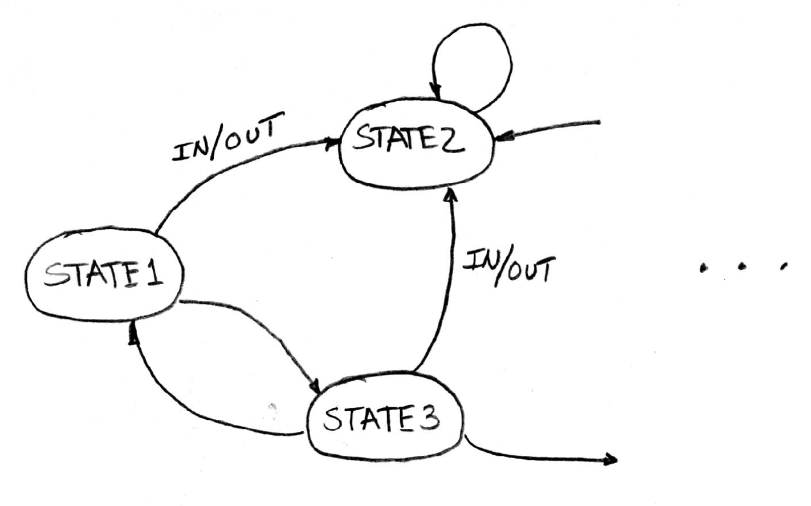
Figure 1:Three state FSM diagram with transition arcs and a self-loop.
3Example: Three One’s
Given combinational logic circuits and registers, FSMs can be implemented in hardware. As an example, let’s consider a small circuit that is used to detect the occurrence of three 1’s in a row in an input sequence of bits.
3.1Waveform Diagram
In this circuit, we assume single bit values are applied one per cycle to the input of the FSM, as shown in the timing diagram in Figure 2. On the cycle when the third 1 of a string of three 1’s appears at the input of the FSM, the machine’s output changes to a 1 for one cycle. After, the output returns to 0 until the FSM detects another string of three 1’s.
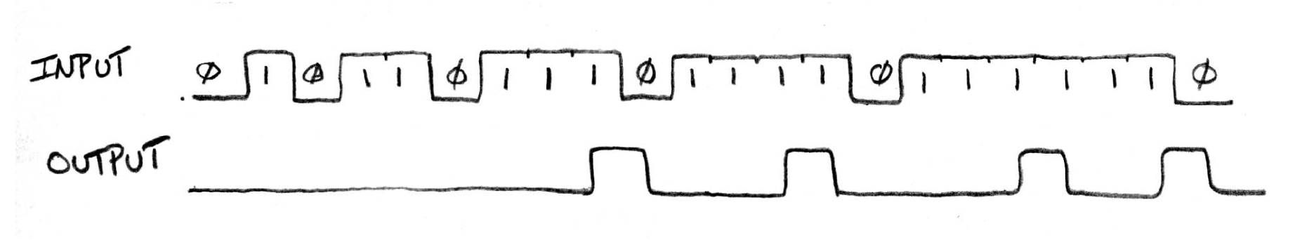
Figure 2:Input and output timing diagram for a circuit detecting three sequential 1 bits.
3.2Finite State Machine
To design the FSM for this example circuit, we start by drawing the state diagram.
The
S0state is the state the machine is in when it begins counting 1’s. This occurs both at the beginning of the sequence, and every time the machine resets and begins looking for a sequence of three 1’s again.The
S1state is the state the machine is in when it has seen one1.The
S2state is the state the machine is in when it has seen two sequential1bits.
In state S0, if the machine sees a 1, it transitions to state S1 with 0 output. If the machine sees a 0, there is a self-loop and it remains in S0 with 0 output.
In state S1, if the machine sees a 1, the output still remains 0 and the machine transitions to state S2. If the machine sees a 0, it resets, returning to state S0 with 0 output.
In state S2, if the machine sees another 1, then the output is changed to a 1 and the machine resets, returning to state S0. If the machine is in state S2 and it sees a 0, then the output remains 0 and the machine resets, returning to state S0.
Using the states and state transitions identified above, we can draw the FSM state diagram (Figure 3) with labeled states and labeled transition arcs.
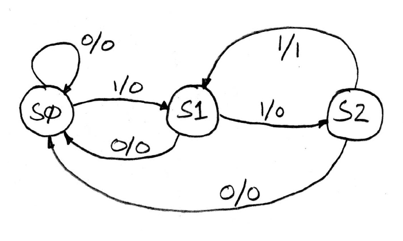
Figure 3:Complete FSM state diagram for three-state circuit detecting three sequential 1 bits.
3.3Truth Table
Using the FSM state diagram we drew above (Figure 3), we can now construct a truth table for our example circuit. To map our state diagram to the truth table, we use the bit patterns 00, 01, and 10, for states S0, S1, and S2, respectively.
The left half of the table shows the present state (PS), also called the current state, and the input value. The right half of the table shows the resulting next state (NS) and output value. Table 1 shows the truth table for our example sequence detecting circuit.
Table 1:Three-1’s Circuit Truth Table.
| PS | INPUT | NS | OUTPUT |
|---|---|---|---|
00 | 0 | 00 | 0 |
00 | 1 | 01 | 0 |
01 | 0 | 00 | 0 |
01 | 1 | 10 | 0 |
10 | 0 | 00 | 0 |
10 | 1 | 00 | 1 |
3.4Circuit
In the hardware implementation of a FSM, we assume that the state transitions are controlled by the clock.
On each clock cycle, the machine:
Checks the inputs
Transitions to a new state
Produces a new output
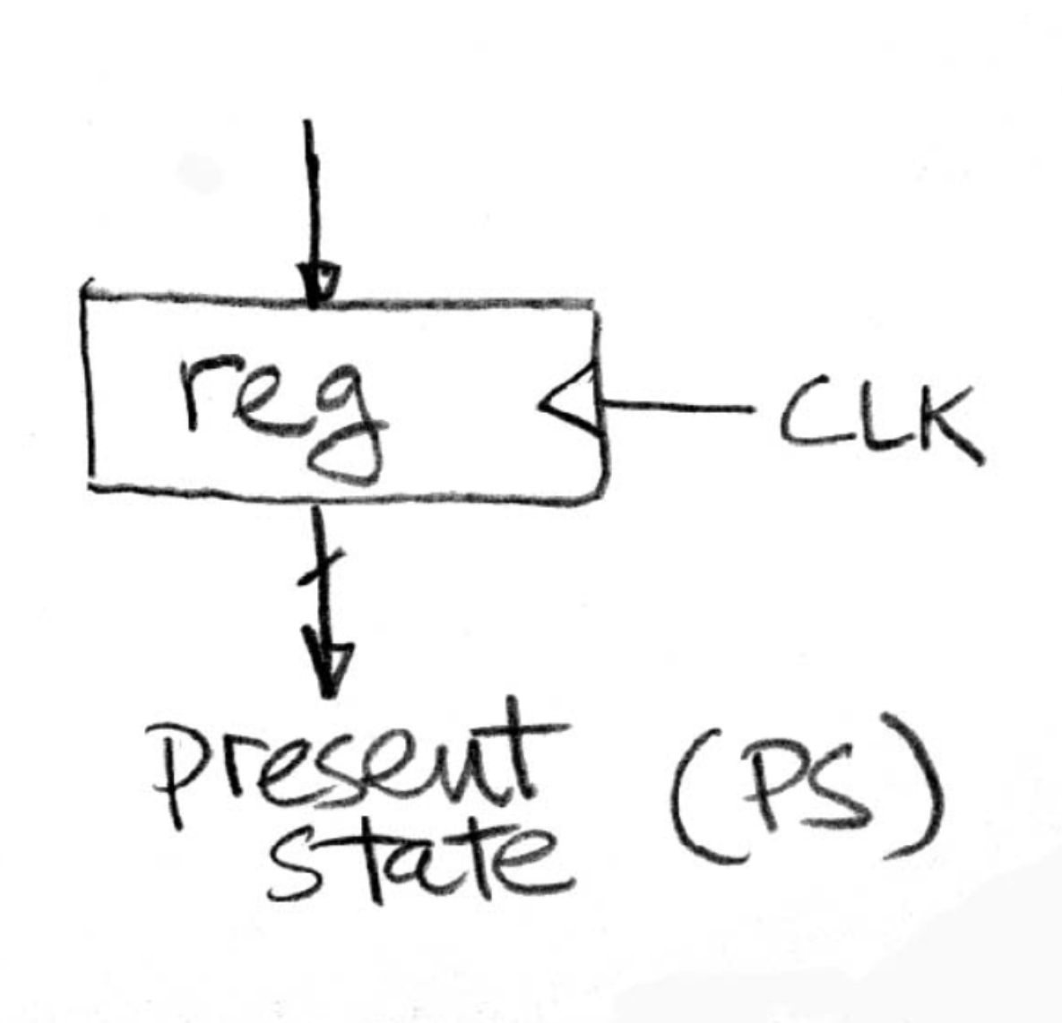
In order to do these steps, we need a register (Figure 4) to hold the current state of the machine. We assign a unique bit pattern, as in the truth table, for each of the states in the state diagram. The register can then keep track of which state the machine is currently in by holding the bit pattern corresponding to the particular state.
Next, we need to design a circuit that implements a function to map the input and present state to the next state and output, as outlined in the truth table in Table 1. We can use a combinational logic circuit (Figure 5) since this circuit doesn’t need to remember anything on its own.
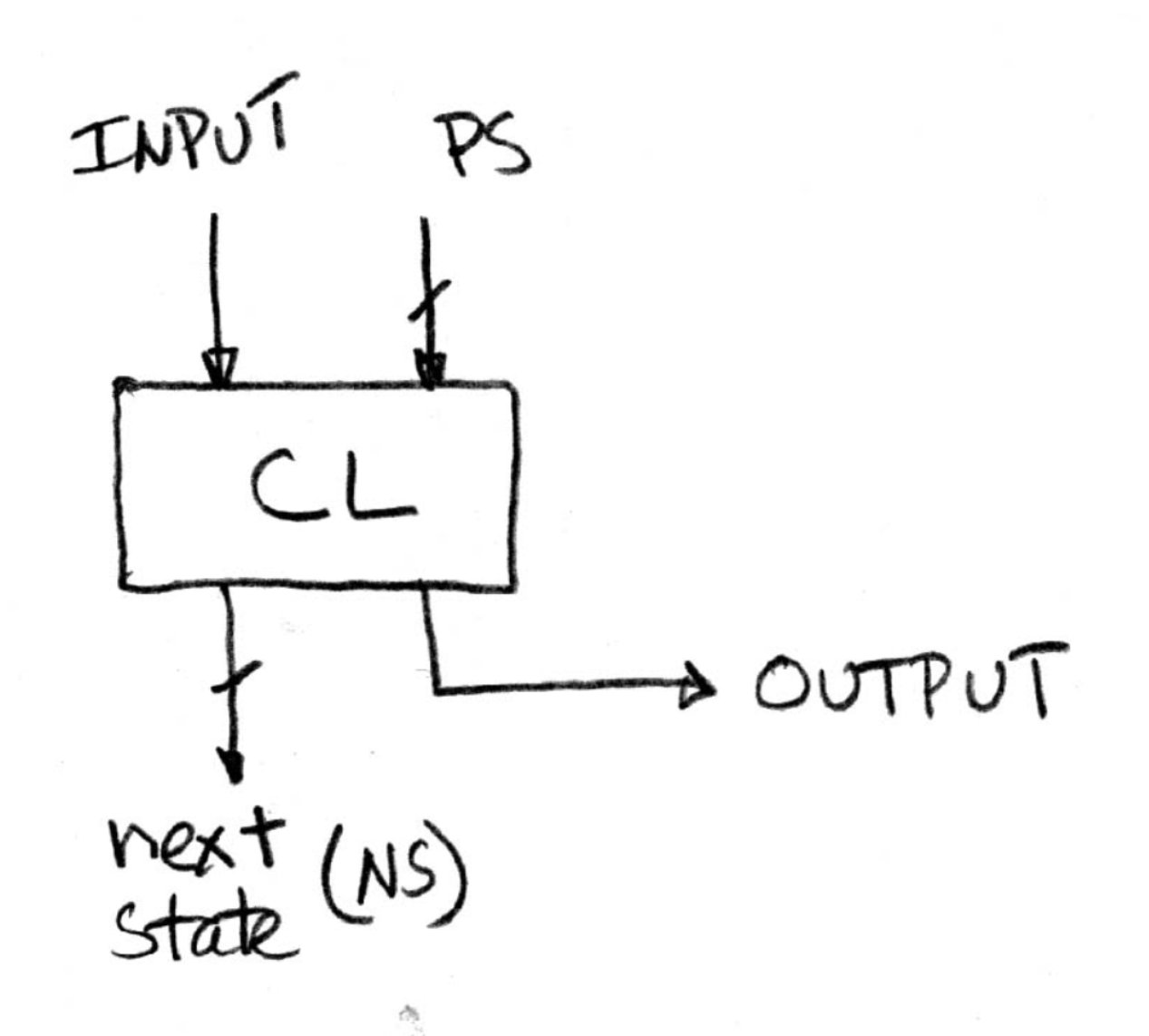
Recall that input bits are applied to the FSM one per clock cycle. Therefore, we want to force a state transition on each clock cycle and can put the combinational logic block in a loop with the state register as shown in Figure 6.
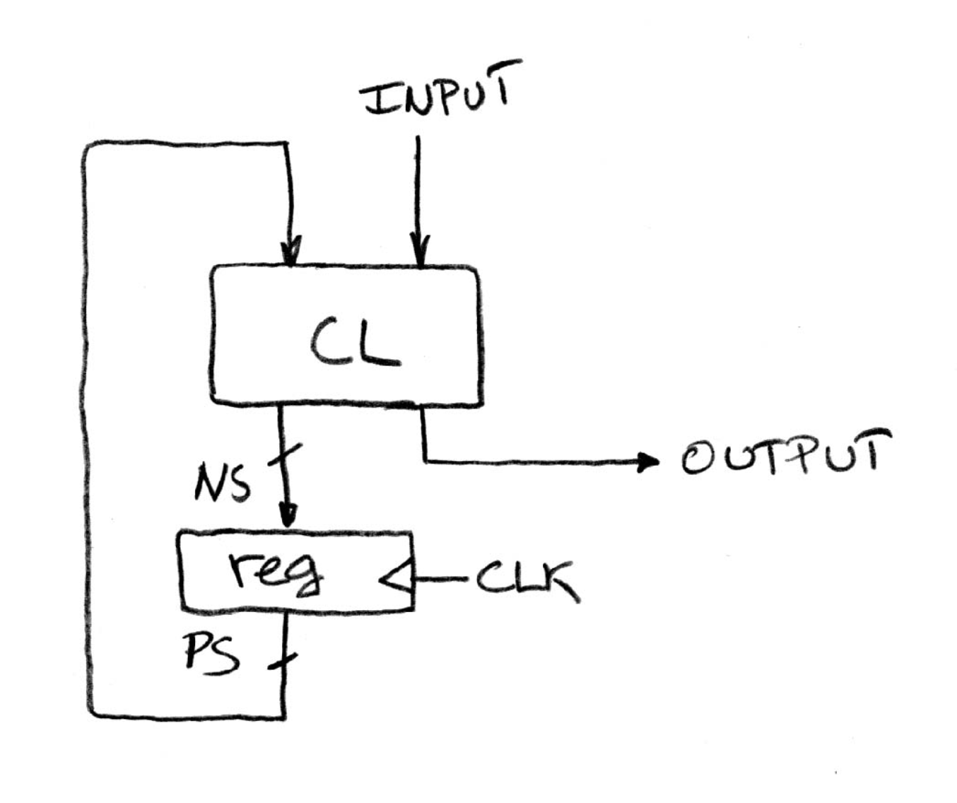
Figure 6:State register and combinational logic implementation of example sequence detector circuit.
On each clock cycle, the combinational logic block looks at the present state and input value to produce the bit pattern for the next state and value of the output (0 or 1). On the rising edge of the clock, the new state value is captured by the register and the process starts again.
These notes are adapted from Professor John Wawrzynek’s notes: State Handout.